
记录生活、工作中碰到的各种问题及解决方式,俗话说“温故而知新,可以为师矣”。解决一系列问题的同时,也是一种成长,故将其进行记录,举一反三,以免重蹈覆辙,本文持续更新。
1、J-Link的灯变成红色(闪烁)表示芯片一直处于复位状态(CC3200 nReset引脚低电平)?
最近把自己画的CC3200 + TM53 Lora模块测试版焊好调试,接上J-Link显示灯一直是红色的,程序理所当然下不进去了,后来发现其复位脚一直处于低电平,且其他IO引脚电压状态不稳定,正是由于用的芯片电压检测芯片CAT811TTB1-GT3复位引脚输出低电平所致。使用RC复位或者利用上拉可以确保有效复位。
2、uniflash无法擦除SPI flash?
虽然参考了TI 推荐的电路,实际制作的板子在使用uniflash擦除SPI flash时,出现以下问题:
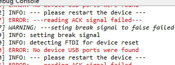
经过监控串口数据发现,原因在于CC3200无法发送相关应答信号,造成后续操作无法进行。
具体原因分析:
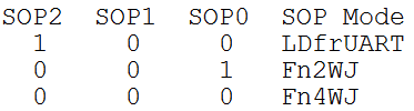
① SOP模式是否正确,SOP分别对应着三种不同的模式,具体如下所示:
② CC3200内部ROM中启动后Bootloader模式使用Pin55、Pin57–UART0进行 程序的下载。
③ Voltage on VDD_ANA1 should be around 1.9V
Voltage on VDD_DIG1 should be around 1.2V
Voltage on VDD_ANA2 should be around 3.3V
④ Reset可能需要注意具体高低电平电压
⑤ SPI Flash芯片是否是CC3200指定的兼容的Flash,否则无法进行烧写与擦除
实际一一调试排查之后,虽然SPI Flash指令是兼容的,由于自己的板子更换了更大容量的Flash造成无法擦除,换回推荐容量的Flash一切正常!!
3、from sgmllib import SGMLParser
ModuleNotFoundError: No module named ‘sgmllib’ 怎么办?
sgmllib是2.6以后引入python,在3.0以后这个库被移除了。如果你的python版本<2.6或者>=3.0就找不到这个module。解决方法:
推荐使用LinkExtractor代替,它比SgmlLinkExtractor更快,而且兼容python3
from scrapy.linkextractors import LinkExtractor
4、SVN Cleanup时遇到错误信息:Cleanup failed to process the following paths: xxxxxxxxx Previous operation has not finished: run ‘cleanup’ if it was interrupted Please execute the ‘Cleanup’ command.
解决方法及步骤:
step 1:下载 Sqlite3.exe (选择sqlite-tools-win32-x86-3200100.zip),解压 后将Sqlite3.exe放到 .svn 的同级目录
step 2:在cmd控制台中将盘符转到svn版本控制的文件夹
step 3:执行sqlite .svn/wc.db “select * from work_queue”
step 4:显示work_queue中保存的工作队列
step 5:执行sqlite3 .svn/wc.db “delete from work_queue”删除工作队列
step 6:重新执行Cleanup命令,It is done!!!
6、Warning “No_connect”
#1 Warning [ALG0047] “No_connect” property on Pin “P1.8” ignored forP1: SCHEMATIC1, 13)URAT (7.90, 1.20). Connecting pin to net “N16811229”.&H)K]‑hwM
$k3D3pd‑T$W7he
ALG0047,这个警告基本可以忽略;造成这个问题的原因是,设计之初先对器件相关的管脚上加上’X'(也就是NC符号),更新设计的过程又对管脚做了连接处理;但是后面的连接处理没有去掉管脚的NC属性,不信的话把那个管脚上的net删掉看看。
解决办法很简单,对这些管脚再做一次NC
7、Warning Part Name
#5 Warning [ALG0016] Part Name “CAP PN_C100UP-6.3V-SMT-S_100UF/6.3V” is renamed to “CAP PN_C100UP-6.3V-SMT-S_100UF/”
这个警告不可避免,allegro对相关的属性名称进行合并,超过一定数量的字符就截掉;在命名规范的前提下就不考虑这个警告了。
无法根治
这个#2 Warning [ALG0016] Part Name “?j#w?rm
之类的错误在于你建立元件原理图的时候你的原件Value值太长了超过32个字符,从而使系统在进行命名规范的时候溢出,而出错,很简单的,只写关键元件名,比如 A2541P10_HDR2X5-100MIL_2X5 HEADER” is renamed to “A2541P10_HDR2X5-100MIL_2X5 HEAD错误只需要
把2X5 HEADER更改为A2541P10,去除中间的空格即可.
U(ZE0B5L5b%X;n4g Allegro对一些字符[例如”空格”,”小数点“等等]很在意,可以参阅相关文档的描述.
8、Error Illegal character “Dot(.)” found in “PCB Footprint”
#1 Error [ALG0081] Illegal character “Dot(.)” found in “PCB Footprint” property for component instance C255: PG16_AC97, PG16_AC97 (226.06, 132.08) .
封装命名不能包含“.”
9、Error Illegal character “Forward Slash(/)” found in “PCB Footprint” property
#1 Error [ALG0081] Illegal character “Forward Slash(/)” found in “PCB Footprint” property for component instance C255: PG16_AC97, PG16_AC97 (226.06, 132.08) .
#2 Error [ALG0081] Illegal character “Forward Slash(/)” found in “PCB Footprint” property for component instance D3: PG01_LED&Switch&7-Segment Disp, PG01_LED&Switch&7-Segment Disp (93.98, 33.02) .
#3 Error [ALG0081] Illegal character “Forward Slash(/)” found in “PCB Footprint” property for component instance C245: PG16_AC97, PG16_AC97 (205.74, 35.56) .
封装命名不能包含“/”
10、比较隐藏的排除法
Loading… E:\FPGA\SCH\allegro/pstchip.dat
#34 WARNING(SPCODD-34): Expected ‘;’ character on line 5308. Check the name and value syntax for invalid characters in the
primitive definition before the line number.
ERROR(SPCODD-47): File ./allegro/pstchip.dat could not be loaded, and the packaging operation did not complete. Check the pxl.log file for the errors causing this situation and package the design again.
#53 ERROR(SPCODD-53): Packaging cannot be completed because packaging has encountered a null object ID. The design may not have been saved correctly. Save the schematic and rerun packaging.
#187 Error [ALG0036] Unable to read logical netlist data.
Exiting… “D:\Cadence\SPB_16.2\tools\capture\pstswp.exe” -pst -d “E:\FPGA\SCH\motherboard.dsn” -n “E:\FPGA\SCH\allegro” -c “D:\Cadence\SPB_16.2\tools\capture\allegro.cfg” -v 3 -j “PCB Footprint”
*** Done*******
掌握排错方法,查找文件pstchip.dat,第on line 5308 看看错误,便可以解决
11、封装命名中不能包含“小数点”、“/”、“空格”,把空格换成下划线或删除,可以解决
********************************************************************************
** Netlisting the design
*********************************************************************************
Design Name:
E:\FPGA\SCH\basicboard.dsn
Netlist Directory:
E:\FPGA\SCH\allegro
Configuration File:
D:\Cadence\SPB_16.2\tools\capture\allegro.cfg
Spawning… “D:\Cadence\SPB_16.2\tools\capture\pstswp.exe” -pst -d “E:\FPGA\SCH\basicboard.dsn” -n “E:\FPGA\SCH\allegro” -c “D:\Cadence\SPB_16.2\tools\capture\allegro.cfg” -v 3 -j “PCB Footprint”
#1 Error [ALG0081] Illegal character “White space” found in “PCB Footprint” property for component instance MG2: Basic, PG06_Stepmotor (180.34, 83.82) .
#2 Error [ALG0081] Illegal character “White space” found in “PCB Footprint” property for component instance ISO1: Basic, PG05_DC Motor (134.62, 40.64) .
#3 Info: PCB Editor does not support Dots(.), Forward Slash(/) and White space in footprint names. The supported characters include Alphabets, Numerics, Underscore(_) and Hyphen(-).
#4 Aborting Netlisting… Please correct the above errors and retry.
Exiting… “D:\Cadence\SPB_16.2\tools\capture\pstswp.exe” -pst -d “E:\FPGA\SCH\basicboard.dsn” -n “E:\FPGA\SCH\allegro” -c “D:\Cadence\SPB_16.2\tools\capture\allegro.cfg” -v 3 -j “PCB Footprint”
*** Done ***
封装命名中不能包含“小数点”、“/”、“空格”,把空格换成下划线或删除,可以解决
12、Warning
#11 Warning [ALG0051] Pin “GND” is renamed to “GND#A6” after substituting illegal characters in Package XC3S1400A-4FG676-C_0FF , U1A: SCHEMATIC1, PG01_FPGACONFIG (2.40, 3.10).
#12 Warning [ALG0051] Pin “GND” is renamed to “GND#A11” after substituting illegal characters in Package XC3S1400A-4FG676-C_0FF , U1A: SCHEMATIC1, PG01_FPGACONFIG (2.40, 3.10).
#13 Warning [ALG0051] Pin “GND” is renamed to “GND#A1” after substituting illegal characters in Package XC3S1400A-4FG676-C_0FF , U1A: SCHEMATIC1, PG01_FPGACONFIG (2.40, 3.10).
#14 Warning [ALG0051] Pin “GND” is renamed to “GND#W8” after substituting illegal characters in Package XC3S1400A-4FG676-C_0FF , U1A: SCHEMATIC1, PG01_FPGACONFIG (2.40, 3.10).
这条警告信息,在命名规范的前提下就不考虑这个警告了。
无法根治,除非去除检测
13、#60 Warning [ALG0016] Part Name “COM_17×2_SIP17X2_COM_17×2” is renamed to “COM_172_SIP17X2_COM_172”.
#61 Warning [ALG0060] No pins are present in J53. Ignoring this component in netlist.
#62 Warning [ALG0016] Part Name “1X3P,MALE,DIP_2.0_SIP3_1X3P_2.54MM” is renamed to “1X3P,MALE,DIP_2.0_SIP3_1X3P_2.5”.
器件管脚不存在,有的器件做了但没放管脚,正常
14、error: Same Pin Number connected to more than one net.
请检查 这个器件的位号是否有重复。 一般是重复了才会出现这种情况。
Checking Pins and Pin Connections
ERROR: [DRC0031] Same Pin Number connected to more than one net. LED&Switch&7-Segment Disp/U17/3 Nets: ‘3V3’ and ‘485_RE/DE’.
PG01_LED&Switch&7-Segment Disp, PG01_LED&Switch&7-Segment Disp (101.85, 73.66)
上面的问题是器件位号重复
15、WARNING: [DRC0008] Two nets in same schematic have the same name, but there is no off-page connector
这个问题是信号同名,到没有用OFF-PAGE连接起来 生成网表会自动重新命名一个名字
16、MSP430编程时常出现的错误
错误1
- Error[Pe127]: expected a statement E:\MSP430\Module\TFT\SD.c 95
- Error[Pe018]: expected a “)” E:\MSP430\Module\TFT\SD.c 132
解决:仔细检查下程序,看有没有一些语法上的错误,多加的“;”就会使程序出现上述错误;或者一些常用语句表达错误。
- Error[Pe130]: expected a “{“
出现问题的原因:
函数声明时缺少分号“;”
- Error[Pe065]: expected a “;”
- 出现问题的原因:
1、函数缺少一个括号“}”
2、if语句少一个括号“}”
17、python 出现以下错误提示:
![]()
原因在于Python源文件unittest.py与系统库名称相同造成的,重新更换名称即可
18、出 Gerber 文件时出现以下提示:
Can’t open parameter file … using default values:
DEVICE-TYPE GERBER6X00
G-CODES NO
STATIONS-PER-WHEEL 24
FILM-SIZE 24000 16000
COORDINATES ABSOLUTE
OUTPUT-UNITS INCHES
FORMAT 5.3
ABORT-ON-ERROR abort film & continue
SUPPRESS-LEAD-ZEROES YES
SUPPRESS-TRAIL-ZEROES NO
OPTIMIZE YES
SUPPRESS-EQUAL YES
SCALE 1.0
1、由于没有设置 光绘文件 路径,通过 Setup -> User Preference -> Paths -> Config -> artpath 进行相关路径设置
2、相关光绘文件目录中不要使用中文,最好使用全英文路径
3、点击 Manufacture -> Artwork -> General Parameters 出光绘文件时就会出现art parameter 参数文件