
This application note explains antenna design in simple terms and recommends two Cypress-tested PCB antennas that can be implemented at a very low cost for use with Bluetooth Low Energy solutions. This application note also provides guidelines for RF component selection, matching network design and layout design.
It is not uncommon to have a wide variation in RF ranges for designs that use the same silicon and the same power but a different layout and antenna-design practice. This application note describes the best practices, layout guidelines, and an antenna-tuning procedure to get the widest range with a given amount of power. Other important general layout considerations for RF trace, power supply decoupling, via holes, PCB stackup, and antenna and grounding are also explored. The selection of RF passives such as inductors and capacitors is covered in detail.
Each topic ends with tips or a checklist of design items related to the topic:
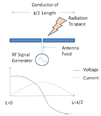
The λ/2-length antenna shown above is called a dipole antenna.
The antenna geometry has two most important considerations:
1、 Antenna length
2、 Antenna feed
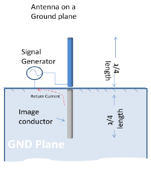
For a quarter-wave antenna that is used in most PCBs, the important considerations are:
1、 Antenna length
2、 Antenna feed
3、 Shape and size of the ground plane and the return path
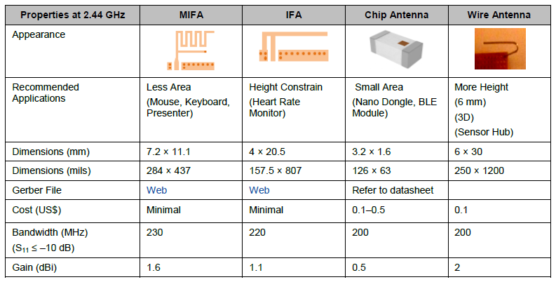
Cypress-Proprietary PCB Antennas
The Meandered Inverted-F Antenna (MIFA) is a popular antenna widely used in human interface devices (HIDs) because it occupies a small PCB area.

Antenna Feed Consideration:
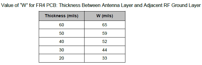
Table below provides the “W” value for different PCB thickness between the top and bottom layers for a two-layer FR4 substrate (relative dielectric constant = 4.3) for coplanar waveguide model. The top layer contains the antenna trace; the bottom layer is the immediate next layer containing the solid RF ground plane. The remaining PCB area of the bottom layer can be used as a signal ground plane.
For the small length of PCB trace that feeds the antenna, the width requirement can be relaxed. Ensure that the antenna trace width and the antenna feed connection have the same width. However, if it is a long transmission line approximately 1 cm from the matching network to antenna or back to the ANT pin of the device, Cypress recommends a transmission line type of layout, having a specific width “W” over a bottom ground plane for the feed.
Antenna Length Considerations
Depending on the PCB thickness, the MIFA antenna should be length-adjusted to adjust the antenna radiation impedance and frequency selectivity. Cypress recommends the values listed in Table below for antenna lengths for various board thicknesses.
Length of MIFA
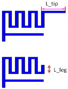
Leg and Tip length
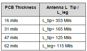
Please note that the original antenna should start with the full length of antenna. Depending on board thickness the antenna needs to be length adjusted. We cannot increase length as easily in a board than cutting the length. Table above should be taken as a guideline to check final length of the antenna for a given board thickness than an exact figure.
The length cutting is a quick method to tune the antenna. If the customer has space to put matching network component and competency for antenna tuning, we recommend putting matching network instead of length adjusting.
Chip Antennas
For applications where the PCB size is extremely small, chip antennas are a good solution.
The following are the major considerations for a chip antenna placement, layout, and RF performance:
1、 Ground clearance around the antenna
2、 Antenna placement for optimal radiation
3、 Antenna feed consideration
4、 Antenna matching network for bandwidth extension
Tips for Matching Network
Use the following tips to minimize the gap between theory and practice in the matching network design:
- Measure the impedance at the same point where components have to be placed.
- Calibrate the network analyzer setup with cables and connectors until the impedance measurement point.
- Place the shunt components on the RF trace itself. Do not use long traces to connect to the shunt components.
- Choose capacitors that have a series resonant frequency at least twice the frequency of operation.
- Choose inductors that have a self resonant frequency at least twice the frequency of operation.
- if the parasitic impedance data is available in the datasheet, use it to derive the actual reactance achievable with that component.
- Use only high-Q components for both capacitors and inductors.
Because the impedance is typically unknown during design time, a design with three components in a π or Tfashion allows you to use all the possible topologies later.
RF Trace Layout Considerations
RF tansmission lines are media that carry RF power from a source to a load through a structured path. Transmission lines need to follow a certain discipline to enable power delivery from source to load with minimal loss. While there are several types of transmission lines, on PCBs, the two most popular types of transmission line are:
- Microstrip line
- Coplanar waveguide (CPWG)
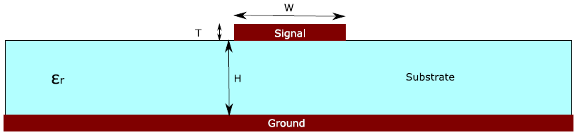
A microstrip line has a signal trace on top of a substrate with a ground plane beneath the substrate. Figure below shows a snapshot of the cross-section of the microstrip line. The following major factors affect the characteristic impedance of a microstrip line:
- Substrate height (H)
- Dielectric constant of the substrate (εr)
- Width of the trace (W)
- Thickness of the RF trace (T)
A CPWG is similar to a microstrip, but it has copper filling on either side of the RF trace with a gap between them, as shown below.
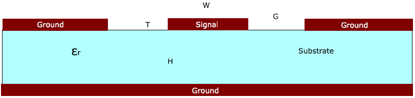
The characteristic impedance of a CPWG depends on the following factors:
- Substrate height (H)
- Dielectric constant of the substrate (εr)
- Width of the trace (W)
- The gap between the trace and the adjacent ground fill (G)
- Thickness of the RF trace (T)
CPWG may be preferred over microstrip for the following reasons:
- It provides a better isolation for RF traces and a better EMI performance.
- It makes it easier to support the grounding of shunt elements on an RF trace.
- It reduces cross-talk with other traces.
- It has a low loss at very high frequencies compared to a microstrip line.
The following are the guidelines for RF trace design:
- Choose the right kind of transmission line (microstrip or CPWG) when calculating the trace width needed for a 50-ohm characteristic impedance.
- Ensure that the RF trace has a 50-ohm characteristic impedance. Use impedance calculators to calculate the trace width and gap needed for a given stackup.
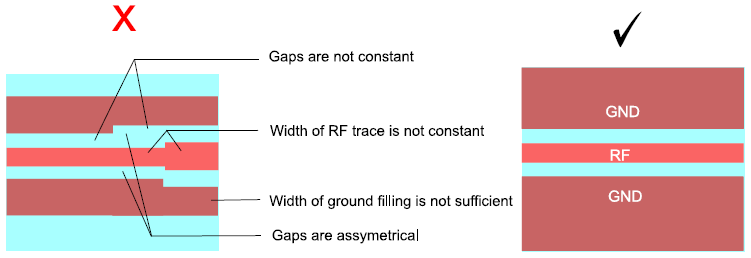
- The characteristic impedance must be constant throughout the trace. Therefore maintain a constant width for the RF trace. For the CPWG, maintain a constant gap between the RF trace and the adjacent ground.
- For the CPWG, ensure that the gap between the grounds in the top layer is less than the height of the substrate; otherwise, the trace will be predominantly microstrip.
- For the CPWG, ensure that the ground pour area on either side of the trace is wider than the gap between the grounds. Some of the commonly made mistakes in the design of RF trace and the correct way to do them are represented in Figure below.
- Ensure a clean, uninterrupted ground beneath the RF trace without any other traces crossing the RF trace to allow a proper return path for the RF currents.
- Maintain the shortest possible length for the RF trace because the traces and the substrate below attenuate the RF signal proportionate to the length.
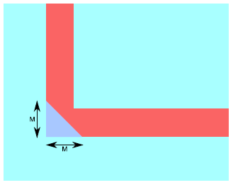
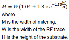
- Avoid bends in the RF trace. If bends are unavoidable, make a curved bend instead of a sharp bend to maintain a uniform width. For a right-angled turn, mitering can be done, as shown below.
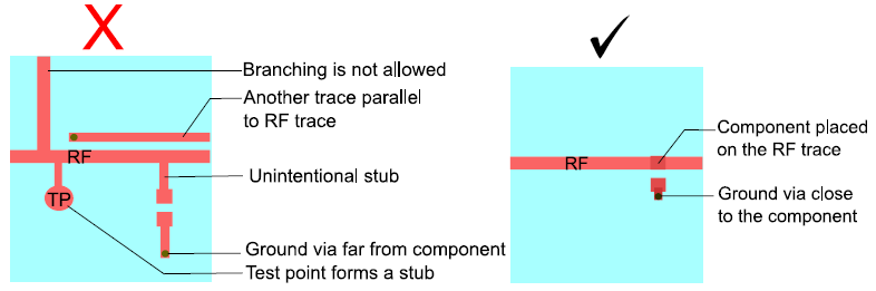
- Avoid stubs or branching in the RF trace. Stubs have reactive impedance and affect impedance matching. While following the reference design, ensure that components are placed on the RF traces in an exact manner as shown in the reference designs. For example, taking a branch from the RF trace to place a shunt component would alter impedance matching; in that case, using the same component value as the one in the reference design may not work in the new design.
- Do not place any other traces close to and parallel to the RF trace. This causes mutual coupling of the signals between traces.
- Do not place test points on the RF trace. They act as stubs and affect impedance matching.
Ground Plane
The ground layer is extremely important in RF PCB design. The return path for the RF signal is in the ground plane beneath the RF trace. For good RF performance, the return path should be uninterrupted and as wide as possible. If the ground plane is interrupted, return currents find the next smallest path around the interruption. This forms a current loop, adding undesired inductance, affecting the impedance match between the radio and antenna, and attenuating the RF signal significantly. If the ground plane beneath the RF trace is narrow, it does not behave like a microstrip and may have more signal leakage.
Ground Plane Considerations:
- Do not have traces running across the RF trace in the ground plane. It is better to keep a layer completely dedicated for ground, even for two-layer PCBs.
- Fill the unused area in the top and bottom layers with ground and connect it with the ground plane with many vias spaced not more than one-twentieth of the wavelength of the operating frequency.
- It is not recommended to use two-layer boards for the CSP package, as the signals need to be brought out through the second layer. This makes the design of an uninterrupted ground plane difficult for RF signals.
- Do not have split grounds unless you can ensure that no current loops are formed in the ground for the current in the return path.
- Allow a wide ground plane beneath the RF trace. Narrow ground planes permit parasitic modes of transmission and increase leakage.
- The bottom ground plane, together with the top ground plane and vias between the two ground planes, ensures that all traces are well shielded. This arrangement significantly improves the EMI and EMC performance.
- It is recommended to cover the corners of the power plane with via holes connecting ground planes on either side of the power plane. This helps to arrest any unwanted EMI emitted from the power plane through board edges.
Power Supply Decoupling
The power supply needs decoupling capacitors to filter out noise from the IC to prevent it from reaching the other sides and vice versa.
Power Supply Decoupling Layout Considerations
Note the following best practices when laying out the power supply traces:
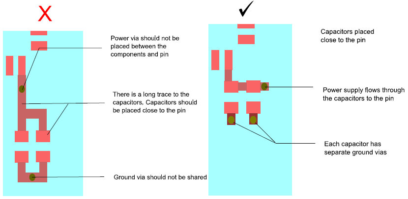
- Place the components as close to the supply pin as possible.
- Place the smallest-value capacitor closest to the power supply pin.
- Place the decoupling capacitor on the same layer as the IC. If it is not possible to place all the capacitors on the same layer, give priority to smaller values.
- The power supply should flow through the decoupling capacitors to the power supply pin of the IC. Avoid using supply vias between the component and the pin.
- Use separate vias to ground for each decoupling capacitor. Do not share vias.
- For four-layer boards with a separate power plane, use separate vias for each power supply pin to the power plane. It is recommended not to share the vias.
- Some of the commonly made layout issues related to power supply decoupling are shown in below.
 Vias
Vias
Vias are critical in enabling signal connectivity across layers in multilayer boards. A ground via placed far from a shunt component changes the impedance of the component seen at the trace, resulting in an impedance mismatch. At high frequency, the parasitic inductance will result in the via having a considerable impedance.
The following guidelines help ensure a proper RF layout:
- Use plenty of vias spaced not more than one-twentieth of the wavelength of the RF signals between ground fillings at the top layer and inner ground layer.
- Place ground vias immediately next to pins/pads in the top layer. Place more vias whenever feasible. More vias in parallel reduce the parasitic inductance.
- Never share a via with multiple pins or pads. Allow separate vias for each pin or pad.
- Avoid using vias to route the RF trace to a different layer.
- Allow a good number of vias for the central ground pad in the QFN package. This minimizes the parasitic inductance and makes the IC see the same ground as the rest of the board.
- Whenever possible, use vias to form a ground fencing around the RF section to isolate it from the rest of the circuit.
A Appendix A: Checklist
- Decide on the PCB antenna type based on the application at hand: MIFA, IFA, wire antenna, or chip antenna.
- Note the chosen antenna layout (dimension).
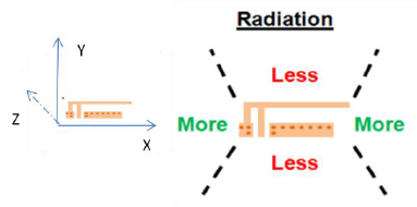
- Orient the antenna suitably for maximum radiation in the desired direction.
- Determine the “W” value to be used in the antenna layout, based on the PCB thickness (stack)
- Select the antenna tip length or leg length for MIFA.
- Check Ground!! This is the Key…Check the Ground clearance for MIFA, IFA or Chip antenna. Check the bottom layer minimum Ground width for better s11. Please look at the layout pictures.
- Make sure that Antenna feed has a solid Gnd plane below it. Make sure that the RF output of the chip is routed like a Tline.
- Do the ID preparation steps for antenna
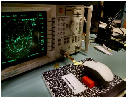
- Calibrate the VNA (one-port calibration is sufficient).
- Measure S11 (dB) with the complete product casing present.
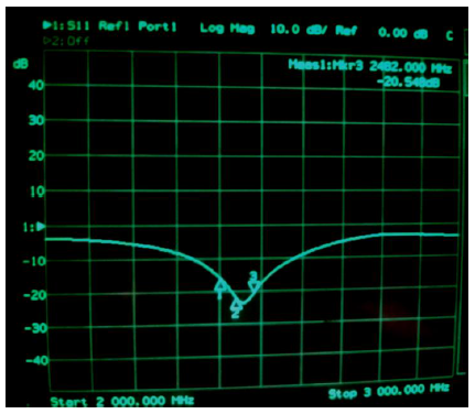
- Tune by matching network S11 (dip) shifts to the desired 2.44GHz with the bare PCB and with complete product casing present.
- Note the final matching network components of the antenna and use them for volume production.
Reference : Antenna_Design_and_RF_Layout_Guidelines