
This series is concerned with the ability of these types of electromagnetic emissions to cause interference in electronic devices. This series is also concerned with the design of electronic systems such that interference from or to that system will be minimized. An electronic system that is able to function compatibly with other electronic systems and not produce or be susceptible to interference is said to be electromagnetically compatible with its environment.
The objective of this text is to learn how to design electronic systems for electromagnetic compatibility (EMC). A system is electromagnetically compatible with its environment if it satisfies three criteria:
- It does not cause interference with other systems.
- It is not susceptible to emissions from other systems.
- It does not cause interference with itself.
Designing for EMC is not only important fro the desired functional performance; the device must also meet legal requirements in virtually all countries of the world before it can be sold. Designing an electronic product to perform a new and exciting function is a waste of effort if it cannot be placed on the market!!!
1、Aspects of EMC
As illustrated above, EMC is concerned with the generation, transmission, and reception of electromagnetic energy. These three aspects of the EMC problem form the basic framework of EMC design. This is illustrated in Fig. 1.
 Figure 1 The basic decomposition of the EMC coupling problem.
Interference occurs if the received energy causes the receptor to behave in an undesired manner. Unintentional transmission or reception of electromagnetic energy is not necessarily detrimental; undesired behavior of the receptor constitutes interference. So the processing of the received energy by the receptor is an important part of the question of whether interference will occur.
It is also important to understand that a source or receptor may be classified as intended or unintended. In facts, a source or receptor may behave in both modes. Whether the source or the receptor is intended or unintended depends on the coupling path as well as the type of source or receptor. This suggests that there are three ways to prevent interference:
- Suppress the emission at its source.
- Make the coupling path as inefficient as possible.
- Make the receptor less susceptible to the emission.
As we proceed through the examination of the EMC problem, these three alternatives should be kept in mind. The “first line of defense” is to suppress the emission as much as possible at the source. In general, the higher the frequency of the signal to be passed through the coupling path, the more efficient the coupling path. So we should slow (increase) the rise / falltimes of digital signals as much as possible. However, the rise / falltimes of digital signals can be increased only to a point at which the digital circuitry malfunctions. This is not sufficient reason to use digital signals having 100 ps rise / falltimes when the system will properly function with 1ns rise / falltimes. Remember that reducing the high-frequency spectral content of an emission tends to inherently reduce the efficiency of the coupling path and hence reduces the signal level at the receptor. Minimizing the cost added to a system to make it electromagnetically compatible will continue to be an important consideration in EMC design.
We may further break the transfer of electromagnetic energy (with regard to the prevention of interference) into four subgroups: radiated emissions, radiated susceptibility, conducted emissions, and conducted susceptibility, as illustrated in Fig. 2. A typical electronic system usually consists of one or more subsystems that communicate with each other via cables (bundles of wires). All of these cables have the potential for emitting and / or picking up electromagnetic energy, and are usually quite efficient in doing so. Generally speaking, the longer the cable, the more efficient it is in emitting or picking up electromagnetic energy. Interference signals can also be passed directly between the subsystems via direct conduction on these cables. It is becoming more common, particularly in low-cost systems, to use nonmetallic enclosures, usually plastic.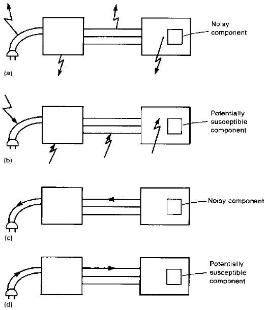 Figure 2 The four basic EMC subproblems: (a) radiated emissions; (b) radiated susceptibility; (c) conducted emissions; (d) conducted susceptibility.
Electromagnetic emissions can occur from the AC power cord, a metallic enclosure containing a subsystem, a cable connecting subsystems or from an electronic component within a nonmetallic enclosure as Fig. 2a illustrates. It is important to point out that “currents radiate”. This is the essential way in which radiated emissions (intentional or unintentional) are produced. A time-varying current is, in effect, accelerated charge. Hence the fundamental process that produces radiated emissions is the acceleration of charge. Although the primary intent of this cable is to transfer 60 Hz commercial power to the system, it is important to realize that other much higher-frequency signals may and usually do exist on the AC power cord!!! To summarize, undesired signals may be radiated or picked up by the AC power cord, interconnection cables, metallic cabinets, or internal circuitry of the subsystems, even though these structures or wires are not intended to carry the signals.
Emissions of and susceptibility to electromagnetic energy occur not only by electromagnetic waves propagating through air but also by direct conducting on metallic conductors as illustrated in Figs. 2c,d. Usually this coupling path is inherently more efficient than the air coupling path. Electronic system designers realize this, and intentionally place barriers, such as filters, in this path to block the undesired transmission of this energy. It is particularly important to realize that the interference problem often extends beyond the boundaries shown in Fig. 2. For example, currents conducted out the the AC power cord are placed on the power distribution net of the installation. This power distribution net is an extensive array of wires that are directly connected and as such may radiate these signals quite efficiently. In this case, a conducted emission produces a radiated emission. Consequently, restrictions on the emissions conducted out the product’s AC power cord are intended to reduce the radiated emissions from this power distribution system.
Our primary concern will be the design of electronic systems so that they will comply with the legal requirements imposed by governmental agencies. However, there are also a number of other important EMC concerns that we will discuss. Some of these are depicted in Fig. 3. Figure 3a illustrates an increasingly common susceptibility problem for today’s small-scale integrated circuits, electrostatic discharge (ESD). Walking across a nylon carpet with rubber-soled shoes can cause a buildup of static charge on the body. If an electronic device such as a keyboard is touched, this static charge may be transferred to the device, and an arc is created between the finger tips and the device. The direct transfer of charge can cause permanent destruction of electronic components such as integrated circuit chips. The arc also bathes the device in an electromagnetic wave that is picked up by the internal circuitry. This can result in system malfunction. ESD is a very pervasive problem today.
After the first nuclear detonation in the mid-1940s, it was discovered that semiconductor devices (a new type of amplifying element) in the electronic systems that were used to monitor the effects of the blast were destroyed. This was not due to the direct physical effects of the blast but was caused by an intense electromagnetic wave created by the charge separation and movement within the detonation as illustrated in Fig. 3b. Consequently, there is significant interest with the military communities in regard to “hardening” communication and data processing facilities against the effect of this electromagnetic pulse (EMP). This represents a radiated susceptibility problem. We will find that the same principles used to reduce the effect of radiated emissions from neighboring electronic systems also apply to this problem, but with larger numbers. Figure 3 Other aspects of EMC: (a) electrostatic discharge (ESD); (b) electromagnetic pulse (EMP); (c) lighting; (d) TEMPEST (secure communication and data processing).
Lightning occurs frequently and direct strikes illustrated in Fig. 3c are obviously important. However, the indirect effects on electronic systems can be equally devastating. The “lightning channel” carries upward of 50000 A of current. The electromagnetic fields from this intense current can couple to electronic systems either by direct radiation or by coupling to the commercial power system and subsequently being conducted into the device via the AC power cord. Consequently, it is important to design and test the product for its immunity to transient voltages on the AC power cord. Most manufacturers inject “surges” onto the AC power cord and design their products to withstand these and other undesired transient voltages.
It has also become of interest to prevent the interception of electromagnetic emissions by unauthorized persons. It is possible, for example, to determine what is being typed on an electronic typewriter by monitoring its electromagnetic emissions as illustrated in Fig. 3d. There are also other instances of direct interception of radiated emissions from which the content of the communications or data can be determined. Obviously, it is imperative for the military to contain this problem, which it refers to as TEMPEST. The commercial community is also interested in this problem from the standpoint of preserving trade secrets, the knowledge of which could affect the competitiveness of the company in the marketplace.
There are several other related problems that fit within the purview of the EMC discipline. However, it is important to realize that these can be viewed in terms of the four basic subproblems of radiated emissions, radiated susceptibility, conducted emissions, and conducted susceptibility shown in Fig. 2. Only the context of the problem changes.
The primary vehicle used to understand the effects of interference is a mathematical model. A mathematical model quantifies our understanding of the phenomenon and also may bring out important properties that are not so readily apparent. An additional, important advantage of a mathematical model is its ability to aid in the design process. The criterion that determines whether the model adequately represents the phenomenon is whether it can be used to predict experimentally observed results. If the predictions of the model do not correlate with experimentally observed behavior of the phenomenon, it is useless. However, our ability to solve the equations resulting from the model and extract insight from them quite often dictates the approximations used to construct the model. For example, we often model nonlinear phenomena with linear, approximate models.
Calculations will be performed quite frequently, and correct unit conversion is essential. Although the trend in the international scientific community is toward the metric or SI system of units, there is still the need to use other systems. One must be able to convert a unit in one system to the equivalent in another system, as in an equation where certain constants are given in another unit system. A simple and flawless method is to multiply by unit ratios between the two systems and cancel the unit names to insure that the quantity should be multiplied rather than divided and vice versa. For example, the units of distance in the English system (used extensively in the USA) are inches, feet, miles, yards, etc. Some representative conversions are 1 inch = 2.54 cm, 1 mil = 0.001 inch, 1 foot = 12 inches, 1 m = 100 cm, 1 mile = 5280 feet, 1 yard = 3 feet, etc. For example, suppose we wish to convert a distance of 5 miles to kilometers. We would multiply by unity ratios as follows:
![]() Cancellation of the unit names in this conversion avoids the improper multiplication (division) of a unit ratio when division (multiplication) should be used. The inability to properly convert units is a leading reason for numerical errors.
Cancellation of the unit names in this conversion avoids the improper multiplication (division) of a unit ratio when division (multiplication) should be used. The inability to properly convert units is a leading reason for numerical errors.
2、Examples
There are numerous examples of EMI, ranging from the commonplace to the catastrophic. In this section we will mention a few of these.
Probably one of the more common examples is the occurrence of “lines” across the face of a television screen when a blender, vacuum cleaner, or other household device containing a universal motor is turned on. This problem results from the arcing at the brushes of the universal motor. As the commutator makes and breaks contact through the brushes, the current in the motor windings (an inductance) is being interrupted, causing a large voltage (L di/dt) across the contacts. This voltage is similar to the Marconi spark-gap generator and is rich in spectral content. The problem is caused by the radiation of this signal to the TV antenna caused by the passage of this noise signal out through the AC power cord of the device. This places the interference signal on the common power net of the household. As mentioned earlier, this common power distribution system is a large array of wires. Once the signal is present on this efficient “antenna,” it radiates to the TV antenna, creating the interference.
A manufacturer of office equipment placed its first prototype of a new copying machine in its headquarters. An executive noticed that when someone made a copy, the hall clocks would sometimes reset or do strange things. The problem turned out to be due to the silicon-controlled rectifiers (SCRs) in the power conditioning circuitry of the copier. These devices turn on and off to “chop” the AC current to create a regulated DC current. These signals are also rich in spectral content because of the abrupt change in current, and were coupled out through the copier’s AC power cord onto the common AC power net in the building. Clocks in hallways are often set and synchronized by use of a modulated signal imposed on the 60 Hz AC power signal. The “glitch” caused by the firing of the SCRs in the copier coupled into the clocks via the common AC power net and caused them to interpret it as a signal to reset.
3、Electrical Dimensions and Waves
Perhaps the most important concept that the reader should grasp in order to be effective in EMC is that of the electrical dimensions of an electric circuit or electromagnetic radiating structure (intentional or unintentional). Physical dimensions of a radiating structure such as an antenna are not important, per se, in determining the ability of that structure to radiate electromagnetic energy. Electrical dimensions of the structure in wavelengths are more significant in determining this. Electrical dimensions are measured in wavelengths. A wavelength represents the distance that a single-frequency, sinusoidal electromagnetic wave must travel in order to change phase by 360°. Strictly speaking, this applies to one type of wave; the uniform plane wave. However, other types of waves have similar characteristics, and so this concept has broad application.
Although Maxwell’s equations govern all electrical phenomena, they are quite complicated, mathematically. Hence we use, where possible, simpler approximations to them such as lumped-circuit models and Kirchhoff’s laws. The important question here is when we can use the simpler lumped-circuit models and Kirchhoff’s laws instead of Maxwell’s equations when analyzing a problem. The essence of the answer is when the largest dimension of the circuit is electrically small, for example, much smaller than a wavelength at the excitation frequency of the circuit sources. Typically we might use the criterion that a circuit is electrically small when the largest dimension is smaller than one-tenth of a wavelength.
This notion of electrical dimensions and lumped-circuit models has other significant aspects that we must discuss. Electromagnetic phenomena are truly a distributed parameter process in that the properties of the structure such as capacitance and inductance are, in reality, distributed throughout space rather than being lumped at discrete points. When we construct lumped-parameter electric circuit models, we are ignoring the distributed nature of the electromagnetic fields. For example, consider a lumped-circuit element such as a resistor and its associated connection leads as shown in Fig. 4. When using lumped-circuit models, we are in effect saying that the connection leads of the elements are of no consequence and their effects may be ignored. When is this valid? In Fig. 4 we have shown the element current (assumed cosinusoidal) that enters the left connection lead and exits the right connection lead as a function of time t. This current is actually a wave propagating with velocity v. If the medium surrounding the connection leads (wires) is air, the velocity of propagation is the speed of light or
![]()
Because of this propagation there is a finite time delay
![]() required for the current wave to transit element and the connection leads and L is the total length of the element and its connection leads. For example, the time delay for a wave propagating in free space (approximately air) over a distance 1 m is approximately 3 ns or about 1 ns per foot. This time delay of propagation is becoming more critical in today’s digital electronic circuits because of the ever-increasing speeds (and consequently the higher frequency content) of those digital signals. For example, in the mid-1980s or so the clock speeds of digital devices were on the order of 10 MHz. These digital signals had rise/falltimes in transitioning from a 1 to 0 and vice versa on the order of 20ns. Today the clock speeds of personal computers are on the order of 3 GHz and the transition times are on the order of 100-500 ps. The velocity of propagation along a printed circuit board (PCB) land that interconnects the components is reduced from that of free space by the presence of the board material that is glass epoxy (FR-4) and is on the order of 1.8 × 10²×10²×10²×10² m/s. Hence the delay in transiting a 6-in. land on that PCB is on the order of 850 ps. Today this propagation delay can be on the order of the rise/falltimes of the digital signal and can cause timing problems in the digital logic. In the mid-1980s it was insignificant, and the delay in transiting the digital gates was the only significant delay problem. Today the interconnect connections are drastically impacting signal integrity. We can look forward to this delay caused by interconnections to become even more critical to the performance of the digital device as clock and data speeds continue to increase seemingly without bound.
required for the current wave to transit element and the connection leads and L is the total length of the element and its connection leads. For example, the time delay for a wave propagating in free space (approximately air) over a distance 1 m is approximately 3 ns or about 1 ns per foot. This time delay of propagation is becoming more critical in today’s digital electronic circuits because of the ever-increasing speeds (and consequently the higher frequency content) of those digital signals. For example, in the mid-1980s or so the clock speeds of digital devices were on the order of 10 MHz. These digital signals had rise/falltimes in transitioning from a 1 to 0 and vice versa on the order of 20ns. Today the clock speeds of personal computers are on the order of 3 GHz and the transition times are on the order of 100-500 ps. The velocity of propagation along a printed circuit board (PCB) land that interconnects the components is reduced from that of free space by the presence of the board material that is glass epoxy (FR-4) and is on the order of 1.8 × 10²×10²×10²×10² m/s. Hence the delay in transiting a 6-in. land on that PCB is on the order of 850 ps. Today this propagation delay can be on the order of the rise/falltimes of the digital signal and can cause timing problems in the digital logic. In the mid-1980s it was insignificant, and the delay in transiting the digital gates was the only significant delay problem. Today the interconnect connections are drastically impacting signal integrity. We can look forward to this delay caused by interconnections to become even more critical to the performance of the digital device as clock and data speeds continue to increase seemingly without bound.
 Figure 4 Illustration of the effect of element interconnection leads.
Suppose that the current and the associated wave are sinusoidal. A sinusoidal propagating wave can be written as a function of time t and position z as (where we have arbitrarily chosen a cosine form)![]() where β is the phase constant in radians per meter (rad/m) and ω = 2πf, where f is the cyclic frequency in Hz. This is shown in Fig. 5 as a function of distance z for fixed times t. As the wave propagates from one end of the connection lead, through the element, and exists the other end of the other connection lead it suffers a phase shift, which is given in (2) by
where β is the phase constant in radians per meter (rad/m) and ω = 2πf, where f is the cyclic frequency in Hz. This is shown in Fig. 5 as a function of distance z for fixed times t. As the wave propagates from one end of the connection lead, through the element, and exists the other end of the other connection lead it suffers a phase shift, which is given in (2) by![]() and l is the total length of the connection leads. The phase shift is alternatively related to wavelength, which is denoted by λ and is the distance that the wave must travel to change phase by 2π radians, which is equivalent to 360°. Hence the wavelength and the phase constant are related by
and l is the total length of the connection leads. The phase shift is alternatively related to wavelength, which is denoted by λ and is the distance that the wave must travel to change phase by 2π radians, which is equivalent to 360°. Hence the wavelength and the phase constant are related by ![]()
Therefore 2 can be written alternatively as ![]() Because distance z appears in this current expression as a ratio with wavelength λ, it becomes clear that physical distance z is not the important parameter; electrical distance in wavelengths z/λ is the critical parameter.
Because distance z appears in this current expression as a ratio with wavelength λ, it becomes clear that physical distance z is not the important parameter; electrical distance in wavelengths z/λ is the critical parameter.
The wavelength of the wave is the distance between successive corresponding points such as the crest of the wave as shown in Fig. 5a. This is similar to observing waves in the ocean. Movement of the wave is ascertained by observing the movement of the crest of the wave as shown in Fig. 5b. The water particles actually exhibit and up – down motion, but the wave appears to move along the ocean surface. In order to track the movement of the wave, we observe the movement of a common point on the wave. For the sinusoidal wave in (2), this means that we track points where the argument of the cosine remains constant:![]() It is also clear that the wave in (2) is traveling in the +z direction since as time t increases, distance z must also increase to keep the argument of the cosine constant in order to track the movement of a point on the waveform. Differentiating (6) gives the velocity of the wave movement as
It is also clear that the wave in (2) is traveling in the +z direction since as time t increases, distance z must also increase to keep the argument of the cosine constant in order to track the movement of a point on the waveform. Differentiating (6) gives the velocity of the wave movement as ![]() Hence the wavelength can be written as
Hence the wavelength can be written as ![]()
 Figure 5 Wave propagation: (a) wave propagation in space and wavelength; (b) wave propagation as time progresses.
Table 1 gives the wavelengths of sinusoidal waves propagating in free space for various frequencies of that wave. Substituting (7) into (2) yields This result illustrates that the phase shift of a wave is equivalent to time delay, which is given by z/v seconds.
Table 1 Frequencies of Sinusoidal Waves and Their Corresponding Wavelengths in Free Space (Air) From (3) and (4) as the current propagates along the connection leads a distance of one wavelength, l = λ, it suffers a phase shift of Φ = βλ = 2π radians or 360°. In other words, if the total length of the connection leads is one wavelength, the current entering the connection leads and the current exiting those leads are in phase but have changed phase 360° in the process of transiting the element. On the other hand, if the total length of the connection leads is one-half wavelength (l = λ/2), then the current suffers a phase shift of 180° so that the current entering the connection leads and the current exiting those leads are completely out of phase. If the length of the connection leads is 1/10th of a wavelength the current suffers a phase shift of 36°. Over a distance of 1/20th of a wavelength it suffers a phase shift of 18°, and over a distance of 1/100th of a wavelength it suffers a phase shift of 3.6°. If the effects of the connection leads are to be unimportant as is assumed by the lumped-circuit model, then the total length of the connection leads must be such that this phase shift is negligible. There is no fixed criterion for this but we will assume that the phase shift is negligible if the lengths are smaller than, say, 1/10th of a wavelength at the excitation frequency of the source. For some situations the phase shift must be smaller than this to be negligible. Physical dimensions are not as important as electrical dimensions in determining the behavior of an electric circuit or device. Electrical dimensions are the physical dimensions in wavelengths.
A physical dimension that is smaller than 1/10th of a wavelength is said to be electrically small in that the phase shift as a wave propagates across that dimension may be ignored. These concepts give rise to the rule of thumb that lumped-circuit models of circuits are an adequate representation of the physical circuit so long as the largest electrical dimension of the physical circuit is less than, say, 1/10th of a wavelength. Table 2 gives the frequencies and corresponding wavelengths for various applications.
Table 2 Frequencies and Corresponding Wavelengths of Electronic Systems
Broadly speaking, the velocity of propagation of a wave in a non conductive medium other than free space is determined by the permittivity ∈ and permeability μ of the medium. For free space these are denoted as ∈0 and μ0 and are given by The units of ∈ are farads per meter or a capacitance per distance. The units of μ are henrys per meter or an inductance per distance. We will see these combinations of units several times in later portions of this text and in a different context. The velocity of propagation in free space (air) is given in terms of these as
 ![]() Other media through which the wave may propagate are characterized in terms of their permittivity and permeability relative to that of free space, ∈r and μr, so that ∈=∈r∈0 and μ = μrμ0. For example, Teflon has ∈r = 2.1 and μr = 1.0. Note that the permeability μ is the same as in free space. This is an important property of nonferrous or nonmagnetic materials. On the other hand, the permeability of sheet steel (a ferrous or magnetic material) is 2000 times that of free space, μr = 2000, whereas it has a relative permittivity of ∈r = 1.0. For nonconductive media, other than free space, the velocity of wave propagation is
Other media through which the wave may propagate are characterized in terms of their permittivity and permeability relative to that of free space, ∈r and μr, so that ∈=∈r∈0 and μ = μrμ0. For example, Teflon has ∈r = 2.1 and μr = 1.0. Note that the permeability μ is the same as in free space. This is an important property of nonferrous or nonmagnetic materials. On the other hand, the permeability of sheet steel (a ferrous or magnetic material) is 2000 times that of free space, μr = 2000, whereas it has a relative permittivity of ∈r = 1.0. For nonconductive media, other than free space, the velocity of wave propagation is ![]() For example, a wave propagating in Teflon(∈r = 2.1, μr = 1) has a velocity of propagation of
For example, a wave propagating in Teflon(∈r = 2.1, μr = 1) has a velocity of propagation of ![]() Dielectric materials (μr = 1) have relative permittivities (∈r) typically between 2 and 12, so that velocities of propagation range from 0.70v0 to 0.29v0 in dielectrics. Table 3 gives ∈r for various dielectric materials. Table 4 gives the relative permeability and relative conductivity (relative to Copper) for various metals.
Dielectric materials (μr = 1) have relative permittivities (∈r) typically between 2 and 12, so that velocities of propagation range from 0.70v0 to 0.29v0 in dielectrics. Table 3 gives ∈r for various dielectric materials. Table 4 gives the relative permeability and relative conductivity (relative to Copper) for various metals.
Table 3 Relative Permittivities of Various Dielectrics Table 4 Relative Permeabilities and Conductivities (Relative to Copper) of Various Metals
 It is very important for the reader to be able to correctly calculate the electrical dimensions of a structure at a particular frequency. The key to doing this is to realize that a dimension of one meter in free space (air) is one wavelength at a frequency of 300MHz. Wavelengths in free space can be easily calculated at another frequency by appropriately scaling the dimension, remembering that one wavelength at 300MHz is 1m. To do this, it is important to realize that as frequency increases, a wavelength decreases and vice versa. For example, a wavelength at 50 MHz is 1 m × 300MHz / 50MHz = 6 m. A wavelength at 2 GHz (1 GHz = 1000 MHz) in air is 300/2000 = 0.15 m = 15 cm. Table 1 gives some representative values.
The electrical dimensions of a circuit or other electromagnetic structure need to be calculated to determine whether it is electrically small (l < 1/10λ). If it is electrically small, we can apply simpler concepts and calculations than would be necessary if it were electrically large (l > 1/10λ). For example, Kirchhoff’s voltage and current laws along with the lumped-circuit modeling of elements are applicable only if the largest dimension of the circuit is electrically small! If the circuit is electrically large, we have no other resource but to use Maxwell’s equations (or some appropriate simplification of them) in order to describe the problem. Clearly, then, it is important to determine the electrical dimensions of a circuit. One can determine this by first calculating the wavelength at the highest frequency of interest and then computing k in relation to l = kλ by writing![]() For example, a circuit or radiating structure whose maximum dimension is 3.6 m and is operated at a frequency of 86 MHz is 3.6/3.49 = 1.03 wavelengths because a wavelength in free space at 86 MHz is 300/86 = 3.49 m. If this structure were immersed in a polyvinyl chloride (PVC) dielectric (∈r = 3.5, μr = 1), its maximum dimension of 3.6 m would be 1.93 wavelengths since the wavelength of 86 MHz in PVC is
For example, a circuit or radiating structure whose maximum dimension is 3.6 m and is operated at a frequency of 86 MHz is 3.6/3.49 = 1.03 wavelengths because a wavelength in free space at 86 MHz is 300/86 = 3.49 m. If this structure were immersed in a polyvinyl chloride (PVC) dielectric (∈r = 3.5, μr = 1), its maximum dimension of 3.6 m would be 1.93 wavelengths since the wavelength of 86 MHz in PVC is 